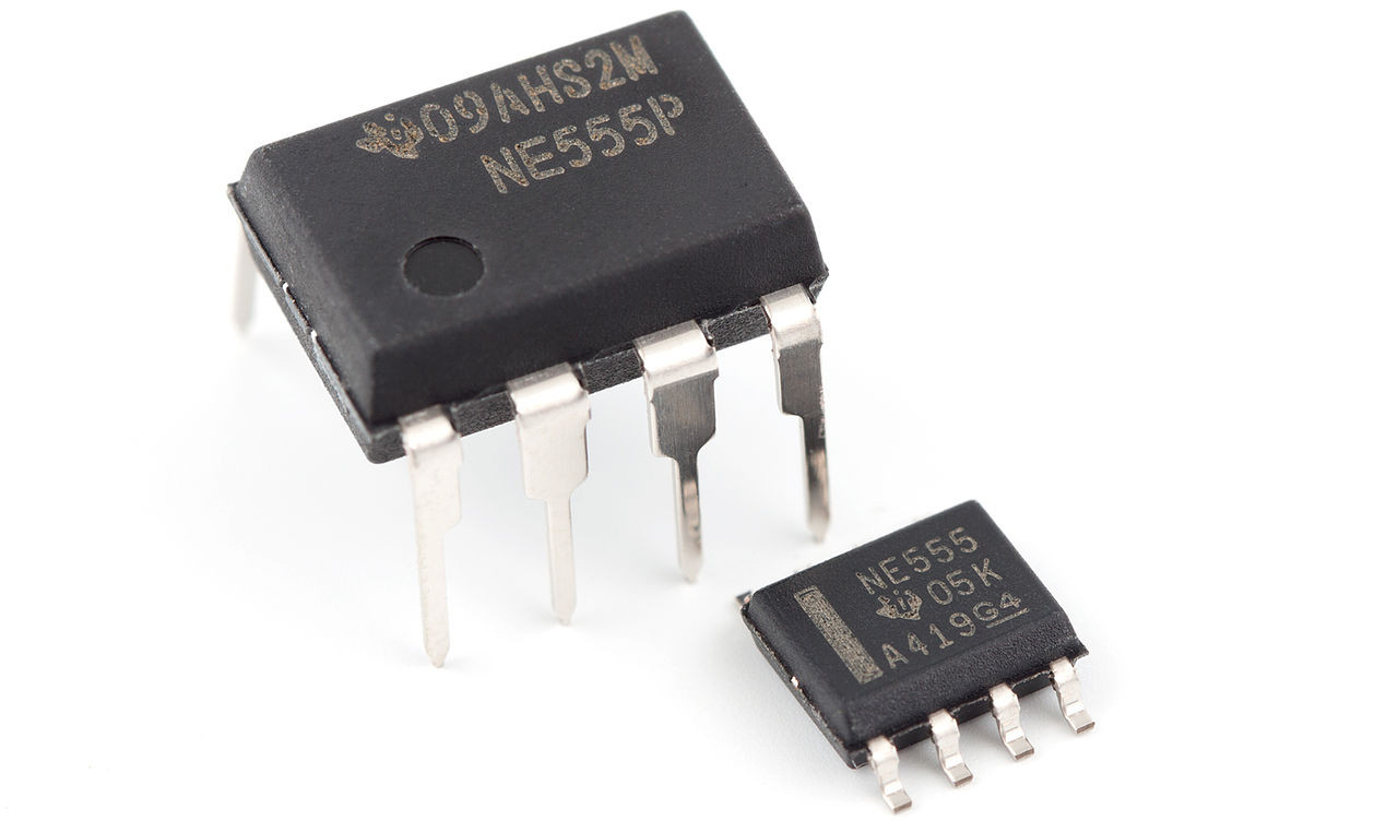
Using the 555 Timer Chip and How it Works
The 555 chip can do two main things:
- Producing time delays (of up to a few minutes). This is called monostable mode.
- Generating repeating digital pulses like a clock signal, typically up to around 1Mhz. This is called astable mode.
How you wire up the chip determines whether it is producing a one-time delay or a repeating clock signal.
Applications
- The 555 can be used to generate sound and it is possible to directly drive a small speaker from the chip. It can produce a single square wave tone at all audible frequencies. It can also produce some sound effects.
- It can be used to control the speed of a motor by turning the motor rapidly on and off. It can also dim light bulbs in the same way and other applications that require control over power delivery to a device.
- It can be used to flash LEDs and other indicators.
- It can be used to turn a device off after a period of inactivity.
How the 555 Works
Despite often being called a "timer", the 555 cannot genuinely produce a time delay on its own. The delay really arises from an external circuit composed of a resistor and a capacitor, an RC circuit, which is a classic method for producing a delay in analogue electronics. What the 555 actually does is control this RC circuit and convert the analogue action into a digital output.
A resistor controls the rate at which electrons can flow in a wire. The greater the value of the resistor, the slower the rate of flow. This is like a pipe controlling a flow of water where reducing the diameter of the pipe can reduce the flow rate of water (as long as the pressure doesn't increase). A capacitor is an electricity storage device and in this analogy is something like a water tank. A tank can store water up to the limit of its capacity and a capacitor can similarly store electrons up to a limit which is determined by the size of the capacitor.
To understand how the 555 works, imagine water continuously flowing into a tank through a pipe. The tank has a drain pipe at the bottom for emptying the contents which is controlled by a valve. The tank contains two sensors that allow a system to detect the level of water in the tank. One sensor is mounted low down to detect a low water level in the tank and the other is mounted higher up to detect a higher level of water in the tank.

The drain valve is initially closed and the tank fills with water. When the high level water sensor goes off, the system opens the drainage valve and the water starts flowing out of the tank. This continues until the low level sensor fails to detect any water present. When this happens the level of water in the tank must be below the height of the sensor. At this point the system closes the valve again. This allows the tank to start filling up with water until the higher sensor again goes off and the cycle repeats.
The system reports when the high level sensor has activated and also reports when the low level sensor fails to detect water. It continuously flips between these two reports. This produces a digital/binary output. We can label a high water level sensor report (meaning the tank is now draining) as a zero and and low level sensor report (meaning the tank is now filling) as a 1.
The 555 represents the system that controls the water tank. In the electronic version, electrons are flowing through a resistor into a capacitor, which gradually fills up with electrons. As the capacitor fills up, the voltage as measured between the capacitor terminals starts to rise. The 555 has a pair of voltage detectors, one of which is set to detect a lower voltage and the other is set to detect a higher voltage. When the higher voltage is detected it drains the capacitor (by sending the electrons in the capacitor to ground). When the voltage goes below the lower level, it shuts off the drainage and the voltage starts building up again in the capacitor. The digital output from the 555 reports a 1 if the capacitor is currently filling (charging) and a 0 if the capacitor is currently draining (discharging) based on the voltage detected.
Inside the 555 chip the two voltage detectors are implemented using components called comparators. These compare two voltages and determine if one voltage is bigger than the other. The comparators are connected to an SR latch circuit which provides the alternating digital output state. The comparators are connected to pins 2 and 6 of the 555 chip. Pin 2 (the trigger) is the lower voltage detector and pin 6 (threshold) is the higher voltage detector.
The oscilloscope trace below shows a real measurement (in yellow) of the voltage output of the RC circuit that goes into the 555 together with the corresponding digital output of the 555 which is shown in blue. The Y axis shows voltage and the X axis shows time. This output is from an astable circuit that is set to produce a frequency of about 20Hz.

The rising and falling RC pulse is converted into a sharply defined digital pulse. When the RC circuit voltage (yellow) is rising, we get a digital 1 out. When when the RC circuit voltage is falling we get a digital 0 out.
The frequency that is output depends on how quickly the capacitor fills with electrons. If the capacitor fills faster then the rate of flipping of the output will be higher, hence a higher frequency is output. There are two mechanisms we can use to control the rate of fill, which are the size of the resistor (controlling the rate of incoming electron flow) or the size of the capacitor, as a larger capacitor will take longer to fill.
Duty Cycle
There is also a third factor that can modify the 555 output and that is the rate of capacitor drainage which is set with an additional resistor. We could have the capacitor fill up quite slowly, but then drain very fast or we could do the reverse and have the capacitor fill up very fast and have it drain very slowly. If the capacitor spends longer filling than draining, then the 555 will spend longer outputting a logic 1 than a logic 0 and the opposite will happen if the capacitor spends longer draining than filling. The proportion of time the 555 spends outputting a 1 compared with a zero is called the duty cycle.
The duty cycle is expressed as a percentage of time spent in the 1 state. A 50% duty cycle means the 555 outputs a 1 and a 0 for the same length of time. A 75% duty cycle, means the 555 spends 3/4 of the time in the 1 state and 1/4 of the time in the 0 state.
If you wanted an LED to occasionally flash e.g. once per 10 seconds, this could be achieved by modifying the duty cycle of an astable circuit such that the 555 spends ten seconds outputting a zero and then perhaps a quarter second outputting a 1.
A common use for duty cycles is to allow the amount of power that is supplied to a device to be varied. For example the speed of a motor can be controlled with an astable circuit by varying the duty cycle of the power supplied to it.
When a motor is running at full speed it has a duty cycle of essentially 100%. There is a logic 1 100% of the time and never a logic 0. Running the motor at half speed can be achieved by setting a duty cycle of 50% (roughly, there are some practical complications that may make the motor not exactly run at half speed). Varying the duty cycle to vary the power supplied to a device is known as Pulse Width Modulation or PWM.
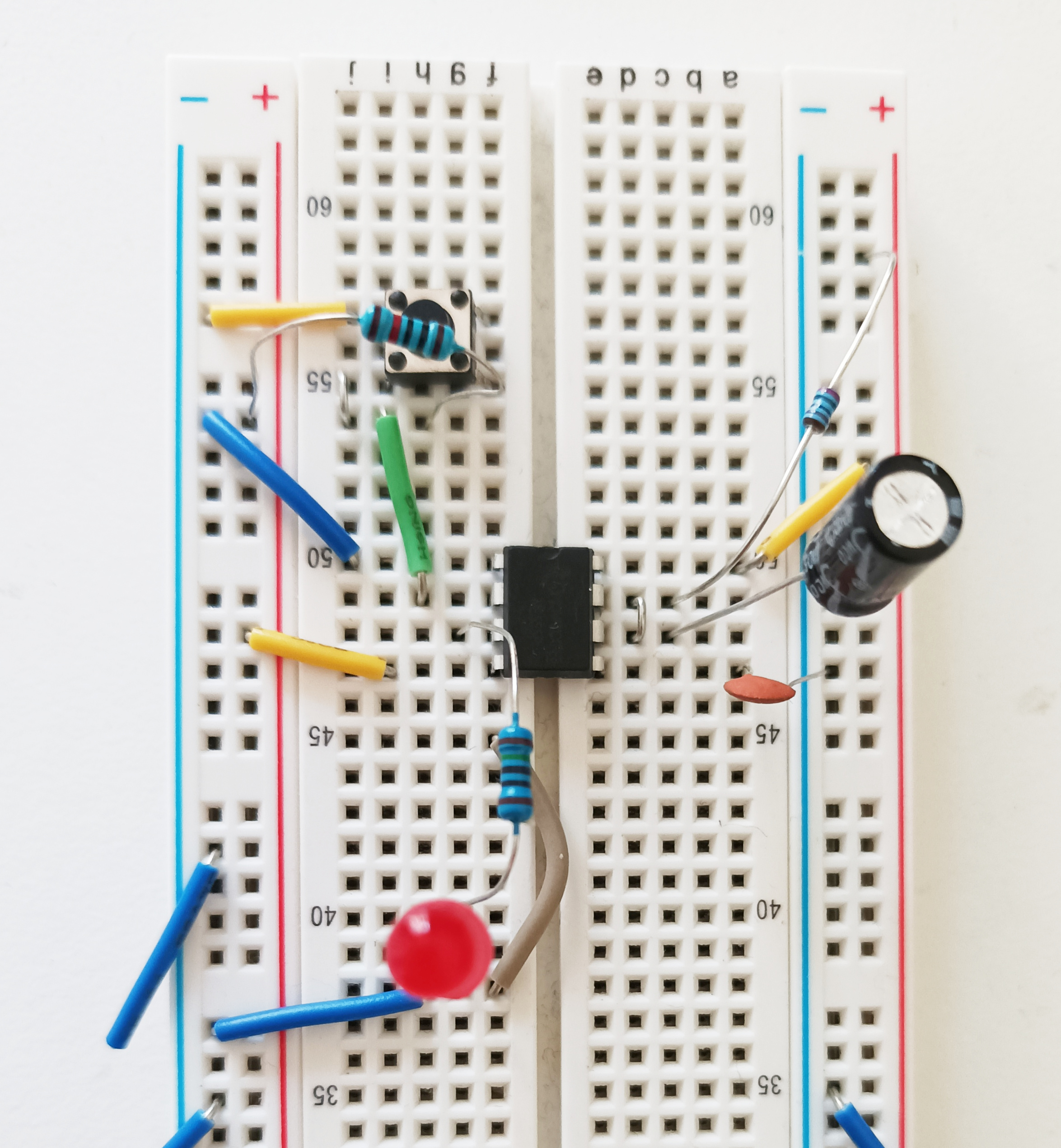
Astable Circuit (Continuous Pulsed Output)
The following circuit produces an output signal at approximately 2Hz i.e. it could be used to flash an LED twice per second. The reason it is not precisely 2Hz is components are only easily available in specific sizes and nearby values to those actually required have been chosen for reasons of practicality.

The following image shows the astable circuit built on a breadboard:

The rate at which the capacitor fills depends on the sum of the values of R1 and R2 and the size of the capacitor. Draining the capacitor is performed by pin 7 on the chip when it internally connects the pin to ground after detection of a high voltage by the comparator. When this happens electrons flow from the capacitor through R2 and then into pin 7. Hence R2 applies a restriction to the draining rate of the capacitor but R1 has no effect on this.
In the astable circuit pins 2 and 6 (the voltage detectors) are both connected to measure the voltage output of the RC circuit with pin 2 detecting if the voltage across the capacitor is low, triggering the capacitor to be refilled and pin 6 detecting is the voltage output is high, causing the capacitor to be drained.
Calculating the Frequency
A formula which shows how long the 555 will spend in the 1 state per cycle is:
T1 = 0.693 x (R1 + R2) x C
That is the sum of the resistances in the RC circuit times the capacitance multiplied by 0.693.
Hence this circuit will spend:
0.693 × ( 5600 + 33000 ) x 0.00001 = 0.267s in the 1 state for each cycle or about a quarter of a second.
The formula for the time spent in the zero state is:
T0 = 0.693 x R2 x C
which is:
0.693 × 33000 x 0.00001 = 0.229s or again around a quarter of a second per cycle in the 0 state.
So this circuit spends approximately a quarter second in both the 1 and 0 states, hence completing a 1 and 0 cycle takes about half a second, so the frequency is about 2Hz. As about the same amount of time is spent in both states, we should expect the duty cycle to be close to 50% (although not quite). The duty cycle is actually about 54%, where it spends very slightly longer in the 1 state.
There is a second capacitor in the circuit which is 10nf on the right connected to pin 5. This capacitor is not involved in the timing at all. This is required by the 555 to suppress noise (errors) in the circuit operation. The value does not usually change.
Monostable Circuit (Timer Function)
In this version of the circuit, the output of the 555 starts out at logic 0 (low) and stays that way permanently until we apply a trigger pulse to the circuit, such as by pressing a button. When we apply the trigger, the 555 output goes to logic 1 (high) for a period of time that is determined by the values of the components in the RC circuit. Then the output goes to zero again and waits until such time as the circuit receives another trigger pulse.
To achieve the monostable version, we essentially change the configuration of pins 2 and 6. Instead of the pins both being connected to the RC output as in the astable version, the trigger (pin 2) is held at a high voltage (the supply voltage) via a 10K resistor. The resistor is just there to prevent a short circuit. The capacitor can't start filling until a low voltage is applied to pin 2. We also connect a button to pin 2 which is connected to ground, which is zero volts. When we press the switch the trigger pin receives the low voltage and the capacitor is then permitted to start filling. The output of the 555 now flips to logic 1 (high).
Pin 6 (the threshold pin) is connected to the RC output and is watching for the higher voltage level appearing at the RC circuit output. When the capacitor reaches a point where it exceeds the upper voltage threshold then the output of the 555 flips to logic 0. It now also activates the discharge (pin 7) which drains the capacitor. However, a difference as compared with the astable version is that pin 2 is prevented from receiving a low voltage indication until such time as we manually press the switch. So the capacitor is preventing from filling again until the button is pressed. There is also no restricting resistor on the capacitor drain rate and so it drains very fast and is available to be filled again almost instantly.
The time delay the circuit provides (in seconds) is calculated as:
T = 1.1 x R1 x C
This particular circuit is set for a time delay of about 1 second.

The following image shows the monostable circuit built on a breadboard:
In monostable mode, delays of more than a few minutes start to become impractical due to the component values needed. To generate long delays, a counter is normally used that is fed with repeating pulses from an astable circuit. The counter produces an output when the count reaches a certain value, representing the required time delay.
Image Credits: 555 Timer Chip Photo, by Swift.Hg, Creative Commons Attribution-Share Alike 3.0 Unported